
AUTO & AV Chip Data Sheet
Features
- Glass Passivation Junction
- Low Forward Voltage Drop
- High Current Capability
- High Reliability
- High Surge Current Capability
- Compatible With Soldering
- Surface Metalization:Ni/Au
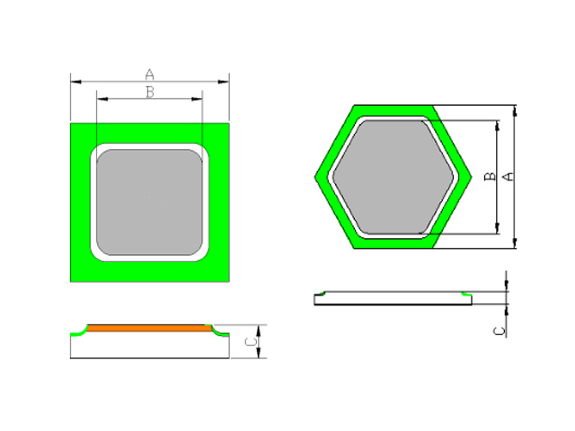
Dimensions
|
Chip size |
A (+1/-2)(mil) |
B(+1/-2)(mil) |
C(±10) |
|
Square |
|
|
|
|
180*180mil |
180 |
155 |
205 |
|
200*200mil |
200 |
176 |
205 |
|
215*215mil |
215 |
191 |
205 |
|
220*220mil |
220 |
196 |
205 |
|
Hexagon |
|
|
|
|
220*220*220mil |
220 |
198 |
205 |
|
240*240*240mil |
240 |
218 |
205 |
Electrical Characteristics (TA=25℃)
|
Parameter |
Symbol |
VALUE |
UNIT |
|
Maximum repetitive peak reverse voltage |
VRRM |
400 for AUTO only |
V |
|
Maximum RMS voltage |
VRMS |
300 for AUTO only |
V |
|
Maximum DC blocking voltage |
VDC |
400 for AUTO only |
V |
|
Maximum average forward rectified current |
IF(AV) |
See Next Table |
A |
|
Maximum instantaneous forwad voltage at IF |
VF |
See Next Table |
V |
|
Peak forward surge current 8.3 ms single half sine-wave superimposed on rated load |
IFSM |
See Next Table |
A |
|
Maximum DC reverse current at rated DC blocking voltage |
IR |
See Next Table |
uA |
|
Maximum reverse recovery time. Test conditions:IF=0.5A, IR=1A, IRR=0.25A. |
Trr |
See Next Table |
ns |
|
Operating tempeterature range |
Tj |
-55~150 |
℃ |
留言咨询
如果您对我们的产品感兴趣,请留下您的电话。
扫码查看公众号